The company claims it is ready to start production lines using Intel's 20A (2nm class) and 18A (1.8nm class) manufacturing methods before TSMC and Samsung Foundry can introduce their own competing manufacturing methods. The company's CEO, Pat Gelsinger, estimates that Intel's 18A manufacturing method – which is expected to be used for mass production in the second half of 2024 – is “slightly ahead” of TSMC's N2 (2nm class) technology expected in the second half. For the year 2025.
Intel intends to use this technology not only for its own products but also for third-party products (IFS or Intel Foundry Services) resulting in a reasonable period of time – as long as timelines are met – gaining an advantage over the strategy. “It has (developed) well Transistor “I have a lot of power,” Pat Gelsinger said in an interview with Barron's. “I think I'm a little ahead of N2, TSMC's next manufacturing method,” he added.
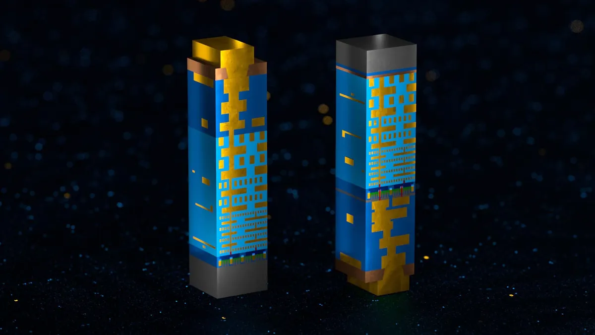
The Intel 20A and Intel 18A manufacturing methods bring two major innovations to semiconductor manufacturing: Gate-All-Around (GAA) RibbonFET transistors and the new PowerVia power delivery design also known as the Backward Power Delivery Network (BSPDN) that we mentioned in the past.
The Intel 20A node is expected to be relatively short-lived, which will allow Intel to learn all the ins and outs of GAA and BSPDN, while the Intel 18A node is intended to be where Intel expects to re-establish its leadership in the semiconductor industry. Hence, the company has pinned a lot of hopes on this particular manufacturing center.
Intel says that Intel's first 18A silicon products are expected to be produced at its factory in the first quarter of 2024, which is in line with expectations that the first products manufactured using this method will be available in the second half of 2024. On the other hand, It will begin manufacturing semiconductors with the N2 method sometime in the second half of 2025. Moreover, although TSMC's N2 method involves nanosheets with GAA-type transistors, it still uses the less efficient traditional method. To save energy, while Intel announced the innovative PowerVIA technology.
However, TSMC still believes that the improved N3P technology, expected in 2024, will provide similar power, performance and transistor density characteristics to Intel's 18A, and claims that N2 is expected to be better across the board than N3P and Intel's manufacturing methods. 18 a. But Pat Gelsinger believes the Intel 18A will have significant advantages over the N2, especially in the performance area thanks to both improved RibbonFET transistors and PowerVIA technology.
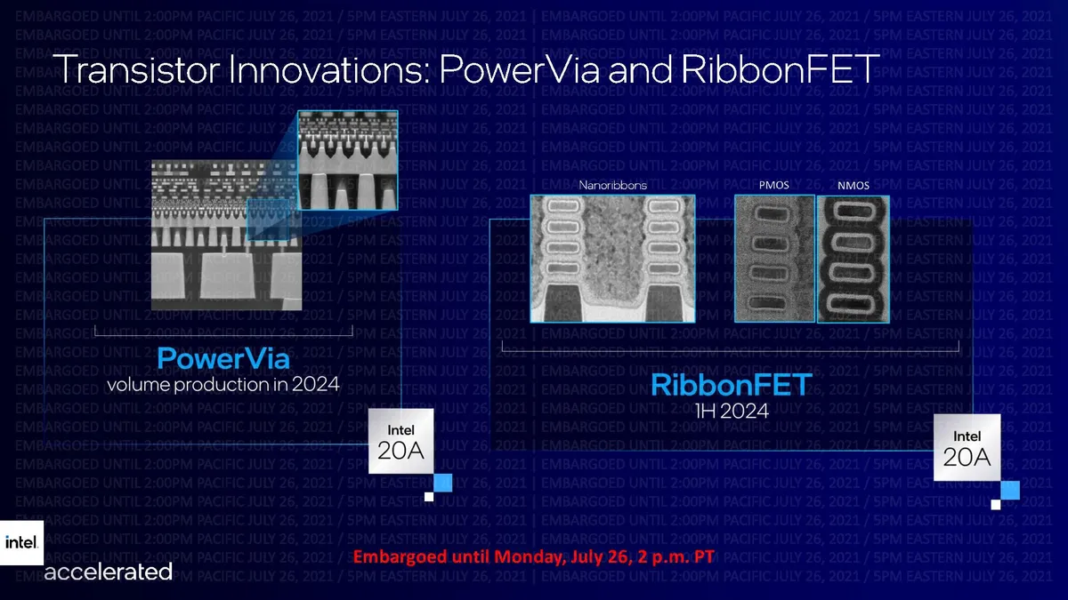
“I think everyone is now at a point where they're looking at and evaluating TSMC's N2 transistor versus our 18A transistor,” Pat Gelsinger said. “There's no evidence yet that one is dramatically better than the other. We'll see who's better. But with PowerVIA, everyone says Intel has gone wild. You're years ahead of the competition they tell us. And it gives us a lot of power. It's Very logical. It provides a better efficiency ratio than the space occupied by silicon, which means lower costs. It also provides better power conduction, which in turn means higher performance.
Pat Gelsinger also hinted that TSMC's N2 could eventually become a very expensive production center, which would give Intel an opportunity with its 20A and 18A manufacturing methods to deliver orders to its factories from customers looking for a higher performance/cost ratio without having to compromise. about their needs. Profit margins.
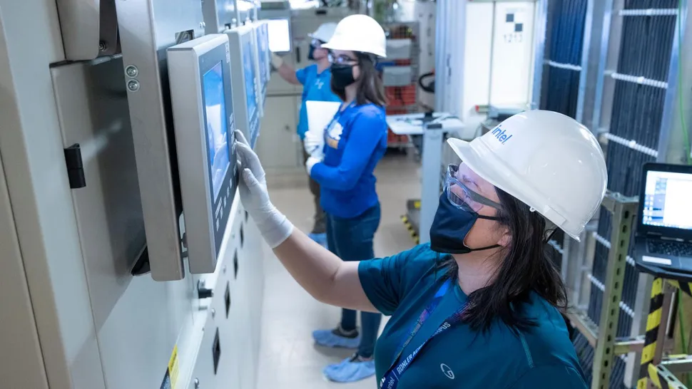
But how has Intel been able to advance so quickly in recent years in manufacturing methods? The answer is complicated, but ASML, based in the Netherlands, played a major role.

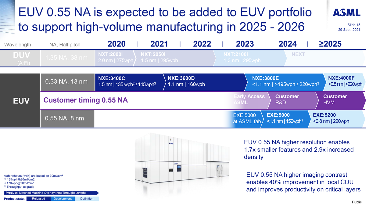
ASML announced that it recently shipped a first-of-its-kind manufacturing unit using extreme ultraviolet (EUV) digital aperture (High-NA) lithography to Intel. This first High-NA machine will be used by the latter to learn all the secrets of the 18A (18 Angstrom, 1.8 nm class) manufacturing method, which promises to give the processor manufacturing giant a significant lead over its competitors (TSMC, Samsung Foundry).
The manufacturing unit is so large that 13 huge containers and 250 boxes were needed to pack and transport it. The machine will be transported from Veldhoven, Netherlands, to Intel's factory near Hillsboro, Oregon, and will be installed there over the next few months. The cost of each of the device's High-NA EUV scanners is estimated at $300 million to $400 million.
The High-NA EUV tool that ASML is sending to Intel is the Twinscan EXE:5000 demo machine that the American company has ordered from ASML since 2018. Intel will use this unit to better understand how to use High-NA EUV tools. EUV for Manufacturing Method 18A is not available and gained valuable experience before ASML developed commercially viable Twinscan EXE:5200 machines that could be used for mass production. Based on reportsIntel intends to purchase six of the ten total modules that ASML will manufacture next year.
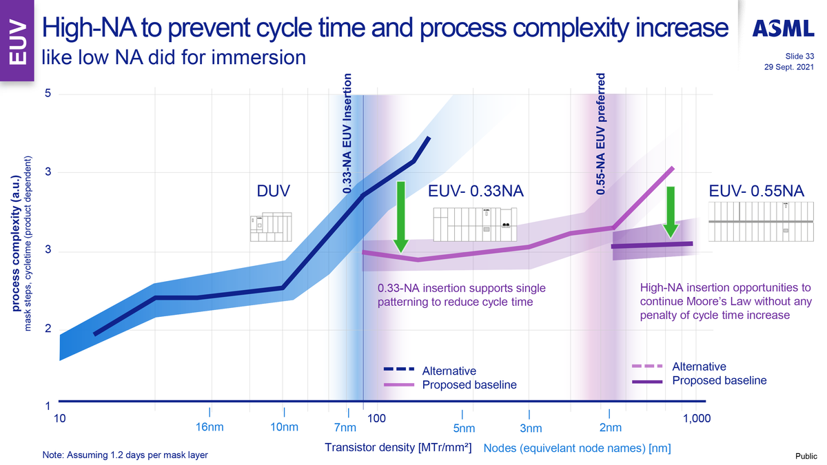
High-NA EUV lithography tools with a 0.55 NA (High-NA) lens can achieve a resolution of 8 nm, a significant advance over standard EUV lithography tools with a 0.33 NA (Low-NA) lens that delivers a resolution of 13 nm. High-NA technology is expected to play a crucial role in 2nm manufacturing methods that will have to use either double EUV Low-NA patterning or single EUV High-NA patterning.
-

5
-
1


“Total alcohol fanatic. Coffee junkie. Amateur twitter evangelist. Wannabe zombie enthusiast.”


More Stories
Apple is gearing up for a partnership that could turn the iPhone upside down
Capcom is removing three of its games from Steam
YouTube is experimenting with showing ads while the video is paused – YouTube